
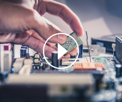
physical design training
Home > Course
physical design training
- Course Duration: 131 Hours
- 4.6 Star (Rating)
- 3000 (Student Enrolled till Now)
- About Course
- Demo Videos
- Course Videos
- Course Curriculum
- Benefits of eLearning?
- Course Instructor
About Course
VLSI Physical Design Training – Complete ASIC Backend Implementation Course
This 8-month Physical Design training program is a comprehensive, industry-oriented course designed to build strong fundamentals and advanced expertise in VLSI Backend Implementation. The program covers the complete ASIC Physical Design flow from Netlist to GDSII with hands-on exposure to real-time projects at 14nm technology node.
The course is structured to prepare freshers, final-year students, and working professionals for careers in Physical Design, ASIC Backend Engineering, Timing Analysis, and Chip Implementation roles in semiconductor companies.
Course Duration & Structure
Foundation Phase – 2.5 Months
Digital Design & Physical Design Fundamentals
Advanced Phase – 5.5 Months
Advanced Backend Implementation with Real-Time Projects
Total Duration: 8 Months Intensive Industry Training
Foundation Training – Digital & Backend Fundamentals
- Digital Design fundamentals (Combinational & Sequential logic)
- CMOS basics and semiconductor concepts
- ASIC Design Flow overview
- Introduction to Physical Design stages
- Understanding Netlist to GDSII flow
- Linux basics for VLSI engineers
- TCL scripting fundamentals
- Static Timing Analysis (STA) basics
Advanced Physical Design Implementation
- Floorplanning and Block-Level Planning strategies
- Power Planning and Power Grid Design
- Standard Cell Placement and Optimization
- Clock Tree Synthesis (CTS) and Clock Optimization
- Global & Detailed Routing strategies
- Congestion Analysis and Routing Debug
- Setup and Hold Violation Debugging
- Timing Closure Techniques
- Multi-Corner Multi-Mode (MCMM) timing analysis
- IR Drop and Electromigration (EM) awareness
- Physical Verification basics (DRC / LVS concepts)
- Low Power Design Implementation overview
- Signoff Flow understanding before Tapeout
Industry Tools Exposure
- Synopsys ICC2 – Complete Physical Design Implementation Flow
- Cadence Innovus – Block & Full-Chip Backend Implementation
- PrimeTime – Static Timing Analysis and Timing Signoff
- Debugging real-time timing violations and optimization strategies
Hands-On Project Experience
Students work on complete backend implementation projects at 14nm technology node, covering the full Physical Design cycle:
- Block-Level Physical Design Project
- Timing Closure Project
- Full flow implementation from Netlist to GDSII
- Real-time routing and timing debug scenarios
Training Modes Available
- Classroom Training
- Live Online Instructor-Led Training
- Weekend Batches
- Fast-Track Programs
- Self-Paced E-Learning
Flexible training options make this course suitable for both fresh graduates and working professionals without interrupting academic or job schedules.
Who Should Enroll?
- ECE / EEE Graduates
- Final-Year Engineering Students
- Freshers targeting Physical Design roles
- RTL Engineers transitioning to Backend
- Working Professionals upgrading ASIC implementation skills
Career Opportunities After Completion
- Physical Design Engineer
- ASIC Backend Engineer
- PD Implementation Engineer
- Timing Engineer
- STA Engineer
This 8-month Physical Design training equips students with practical, tool-based backend expertise required by semiconductor and VLSI companies, ensuring strong career growth in ASIC and chip implementation domains.
| Unit Number | Topic | Duration(mins) |
| 1 | Introduction to digital system | 24 |
| 2 | Number system introduction and Radix conversion | 60 |
| 3 | Compliments of the number systems and 1 s and 2 s Compliments | 92 |
| 4 | 9 s and 10 s Compliments, 7 s and 8 s Compliments and 15 s and 16 s Compliments | 64 |
| 5 | Gates and its truth table and Why NAND is preferred over NOR gate | 71 |
| 6 | NAND and NOR Realization | 66 |
| 7 | SOP and POS form, minterm, Maxterm canonical SOP and POS form | 55 |
| 8 | Boolean equations Switching equations | 25 |
| 9 | Boolean minimization techniques and K -map(2-variables,3-variables,4-variables) and Logisim tool introduction | 99 |
| 10 | Implicants, PI, EPT, NEPT and RPI | 54 |
| 11 | K -map(5-variables,6-variables) | 25 |
| 12 | K -map with don t care functions | 26 |
| 13 | Building of combinational logic circuits (code converters) | 49 |
| 14 | Code converters continues | 43 |
| 15 | Arithmetic circuits (HA, FA and Parallel Adder) | 63 |
| 16 | Subtractors using compliments (HS, FS) | 61 |
| 17 | MSI circuits (Multiplexers) and Gates using Muxs | 66 |
| 18 | Boolean function Implementation using Mux | 53 |
| 19 | FA using Mux and Mux tree | 61 |
| 20 | Demultiplexers | 41 |
| 21 | Decoders | 40 |
| 22 | Decoders configurations and priority encoders | 71 |
| 23 | Comparators | 56 |
| 24 | Introduction to sequential logic ckts, Basic storage element (NOR latch) | 68 |
| 25 | NAND latch | 44 |
| 26 | Clocked SR latch, Clocked D latch, Clocked JK latch, Clocked T latch, Racing problems | 83 |
| 27 | Master-Slave combination and Edge triggering Flip flops | 78 |
| 28 | Revision of latch, Clocked SR latch, Clocked D latch, Clocked JK latch, Clocked T latch, Racing problems | 59 |
| 29 | Master-Slave combination and its limitations | 6 |
| 30 | Edge triggering and its advantages | 50 |
| 31 | Asynchronous inputsOverriding inputs of Flip flops, Characteristic equations and Excitation table of Flip flops | 64 |
| 32 | Flip flop conversions | 17 |
| 33 | Applications of the Flip flops (Counters - Asynchronous up and down counters) | 67 |
| 34 | Asynchronous Mod-N counters | 59 |
| 35 | Asynchronous updown counters, Timing considerations of the flip flops and limitations of the Asynchronous counter | 50 |
| 36 | Design of synchronous counters | 87 |
| 37 | Registers, shift registers and its configurations, universal shift registers | 62 |
| 38 | Counters based on shift registers (Ring and Johnson counters) | 51 |
| 39 | Frequency divider circuits | 100 |
| 40 | Frequency multiplier and Edge detector circuits | 35 |
| 41 | Introduction to FSM, Implicit and Explicit FSM | 62 |
| 42 | FSM sequence detector of melay and moore model | 101 |
| 43 | Problems on FSM | 81 |
| 44 | Assignment discussion | 33 |
| 45 | Synchronizers to change the pipelining. | 24 |
| 46 | FSM | 98 |
| 47 | FSM-Mealy and moore problems,doubt discussion | 101 |
| 48 | D Flip flop using transmission gate | 25 |
| 49 | ASIC FLOW SES1 | 164 |
| 50 | ASIC FLOW SES2 | 170 |
| 51 | ASIC FLOW SES3 | 137 |
| 52 | ASIC FLOW SES4 | 170 |
| 53 | SES1 P1 Introduction to Linux and its applications | 27 |
| 53 | SES1 P2 Architecture of the Linux system | 23 |
| 54 | SES1 P3 Usage of the Cygwin | 13 |
| 55 | SES1 P4 File commands of the Linux system | 63 |
| 56 | SES2 P1-5 File commands continue | 65 |
| 57 | SES2 P2-6 File display and Miscellaneous commands | 62 |
| 58 | SES3 P1-7 file display and Miscellaneous commands continue | 43 |
| 59 | SES3 P2-8 Meta characters and regular expressions | 42 |
| 60 | SES4 P1-9 file compare commands | 58 |
| 61 | SES4 P1-10 .bashrc file | 37 |
| 62 | SES7 P1-11 piping, xargs and tee concept | 41 |
| 63 | SES7 P2-12 env variables, PS1, popd and pushd concept | 33 |
| 64 | SES7 P3-13 filters and commands | 35 |
| 65 | SES8 P1-14 Data manipulation(sed) commands | 71 |
| 66 | SES8 P1-15 Data manipulation(awk) commands | 41 |
| 67 | SES9 P1-16 File permission commands | 69 |
| 68 | SES9 P1-17 File compare commands | 106 |
| 69 | SES9 P1-18 Find commands | 43 |
| 70 | Introduction to TCL | 39 |
| 71 | How to run the TCL program | 57 |
| 72 | Formal syntax of the TCL | 49 |
| 73 | set, puts and gets commands | 36 |
| 74 | TCL Operators | 86 |
| 75 | TCL Control statements | 58 |
| 76 | TCL Control statements (if and for statements) | 63 |
| 77 | TCL Control statements (while statements) | 31 |
| 78 | TCL Control statements (switch and foreach statements) | 29 |
| 79 | TCL strings and its operators | 23 |
| 80 | Strings operators Conti... | 67 |
| 81 | Examples of Strings operators Conti... | 63 |
| 82 | Programs on TCL Strings operators | 55 |
| 83 | TCL Lists | 25 |
| 84 | Programs on TCL Lists | 54 |
| 85 | TCL special variables | 60 |
| 86 | Programs on TCL special variables | 29 |
| 87 | Programs on TCL special variables Conti... | 34 |
| 88 | TCL File handling operations | 53 |
| 89 | Programs on TCL File handling operations | 58 |
| 90 | Programs on TCL File handling operations Conti... | 55 |
| 91 | TCL Procedures and Programs on TCL Procedures | 82 |
| 92 | TCL Procedures and Programs on TCL Procedures Conti... | 49 |
| 93 | TCL Procedures and its parameters | 51 |
| 94 | TCL Arrays | 31 |
| 95 | TCL Associative Arrays | 46 |
| 96 | Programs on TCL Arrays | 33 |
| 97 | TCL Dictionary | 64 |
| 98 | TCL Regular expression | 48 |
| 99 | Programs on TCL Regular expression | 47 |
| 100 | Programs on TCL Regular expression Conti... | 45 |
| 101 | Programs on TCL Regular expression Conti... | 60 |
| 102 | Semiconductor Basics | 52 |
| 103 | Semiconductor Basics Part-2 | 6 |
| 104 | Semiconductor Devices - Diodes | 30 |
| 105 | MOSFET operation & Characteristics Part 1 | 78 |
| 106 | MOSFET operation & Characteristics Part 1-->2 | 53 |
| 107 | MOSFET operation & Characteristics Part 2 | 76 |
| 108 | MOSFET operation & Characteristics Part 2-->2 | 11 |
| 109 | Pass transistors | 45 |
| 110 | pass transistor continuation | 30 |
| 111 | Pseudo NMOS | 23 |
| 112 | Transmission gates | 34 |
| 113 | CMOS Inverter | 57 |
| 114 | Designing using Cmos logic | 53 |
| 115 | VT FLAVOURS & TIMING DELAYS | 63 |
| 116 | VT FLAVOURS & TIMING DELAYS Part-2 | 7 |
| 117 | Device Sizing | 51 |
| 118 | Device sizing continuation | 41 |
| 119 | Device sizing continuation Part2 | 29 |
| 120 | Power Dissipation in CMOS | 68 |
| 121 | Continue power dissipation in CMOS | 44 |
| 122 | Short quiz | 7 |
| 123 | Layout | 60 |
| 124 | PD BASICS SES1 | 91 |
| 125 | PD BASICS SES2 | 120 |
| 126 | PD BASICS SES3 | 166 |
| 127 | PD BASICS SES4 | 139 |
| 128 | PD BASICS SES5 | 104 |
| 129 | PD BASICS SES6 | 131 |
| 130 | PD BASICS SES7 | 112 |
| 131 | PD BASICS SES8 | 109 |
Curriculum
Physical Design training
| PD Flow Stage | Synopsys Tool | Cadence Tool |
|---|---|---|
| RTL to Gate Synthesis | Design Compiler (DC) | Genus |
| Floorplanning & Placement | IC Compiler II (ICC2) | Innovus |
| Power Planning | ICC2 / PrimePower | Innovus / Voltus |
| Clock Tree Synthesis (CTS) | ICC2 | Innovus |
| Routing (Global + Detailed) | ICC2 | Innovus |
| Parasitic Extraction (PEX) | StarRC | Quantus QRC |
| Timing Analysis (STA) | PrimeTime | Tempus |
| Signal Integrity (SI) | PrimeTime SI / StarRC | Tempus SI / Quantus QRC |
| Power Integrity (IR/EM) | RedHawk-SC (via ANSYS) | Voltus |
| Formal Equivalence Checking | Formality | Conformal |
| Physical Verification (DRC/LVS/ERC) | IC Validator (ICV) | Pegasus / PVS |
| GDSII Generation | ICC2 | Innovus |
Specification & Design Flow
- Specification
- RTL Coding & Lint Checks
- RTL Integration
- Connectivity Checks
- Functional Verification
- Synthesis & STA
- Gate Level Simulations
- Power Aware Simulations
- Placement and Routing
- DFT
- Custom Layout
- Post Silicon Validation
Transistors in Hardware Design
- Significance of transistors in hardware design
- Logic gate implementation using BJT, CMOS
- MOSFET functionality
Semiconductors
- What makes Semiconductor special element?
- Classification of solids into three types
- Conductor, Insulator, Semiconductor
- Energy bands in Solids
- Types of Semiconductors
- Intrinsic Semiconductors
- Extrinsic Semiconductors
- Types of Extrinsic Semiconductors
- N-type Extrinsic Semiconductor
- P-type Extrinsic Semiconductor
- Si, Ge – comparison
- Types of current in Semiconductors – Drift, Diffusion
- Ion
PN Junction Diode
- PN Junction – forward, reverse bias
- V-I Characteristics of PN Junction Diode
- Different types of Diode
- Applications of Diode
BJT
- BJT
- BJT working principle
- How BJT can be used for large scale manufacturing
- BJT fabrication steps
- Types of BJT
- Why BJT is not used in lower technology nodes
- Issues with BJT
- Advantages of BJT
- NAND gate using BJT
Field Effect Transistor (FET)
- What is Field Effect Transistor?
- Types of FET
- NMOS
- PMOS
- CMOS
- Fin
NMOS
- What is NMOS?
- NMOS working principle
- Different voltages, currents, their equations
- NMOS circuit representation
- How NMOS works like a switch
- How NMOS can be used for large scale manufacturing
- NMOS fabrication steps
- Types of NMOS
- Why CMOS is used instead of NMOS
- Issues with NMOS
- Advantages of NMOS
- NAND gate using NMOS
CMOS
- What is CMOS?
- CMOS working principle
- Different voltages, currents, their equations
- CMOS circuit representation
- How CMOS works like a switch
- How CMOS can be used for large scale manufacturing
- CMOS fabrication steps
- Types of CMOS
- Issues with CMOS
- Advantages of CMOS
- NAND gate using CMOS
- CMOS second order effects
FinFET
- What is FinFET?
- FinFET working principle
- Different voltages, currents, their equations
- Circuit representation
- How FinFET works like a switch
- How FinFET can be used for large scale manufacturing
- FinFET fabrication steps
- Types of FinFET
- Issues with FinFET
- Advantages of FinFET
- NAND gate using FinFET
- FinFET second order effects
- Layers of CMOS
- Depositing Oxide Layer
- Photolithography
- Masking
- Etching Layers
- Formation of N-Well
- Self-Aligned Gate Fabrication Process
- Diffusion to Create N+ and P+ Regions
- Metallization
Combinational Logic
- Number Systems
- Radix Conversions
- K-Maps, Min-terms, Max Terms
- Logic Gates
- Realization of Logic Gates using MUXs and Universal Gates
- Complements (1’s / 2’s / 9’s / 10’s Complement)
- Arithmetic Operations using Complements
- Boolean Expression Minimization, DeMorgan Theorems
- POS and SOP
- Conversion and Realization
- Adders
- Half Adder
- Full Adder
- Subtractors
- Half Subtractor
- Full Subtractor
- Multiplexers
- Realizing Bigger MUXs using Smaller MUXs
- Implementing Adders and Subtractors using Multiplexers
- Decoders and Encoders
- Implementing Decoders and Encoders using MUX and DEMUX
- Bigger Decoder/Encoder using Smaller Decoder/Encoder
- Comparators
- Implementing Multi-bit Comparators using 1-bit Comparator
Sequential Logic
- Latch, Flip-Flop
- Latch, Flip-Flop using Gates or MUXs
- Different Types of Flip-Flops
- Flip-Flop Truth Table
- Excitation Tables
- Realization of Flip-Flops using Other Flip-Flops
- Applications of Flip-Flops and Latches
- Counters
- Shift Registers
- Synchronizers for Clock Domain Crossing
- FSMs
- Mealy and Moore FSM
- Different Encoding Styles
- Frequency Dividers
- Frequency Multiplication
- Static Timing Analysis (STA)
- Setup Time, Hold Time, Timing Closure
- Fixing Setup and Hold Time Violations
- Launch Flop and Capture Flop
- Introduction to majorly used keywords on PD flow
- VLSI Technology concepts
- Resistance, Capacitance, Inductance
- Parasitic capacitance
- L-C-R circuit analysis
- RC circuit significance with circuit delay
- Clock distribution concepts, skew
- Installing Linux platform in Windows
- Linux Basics
- Linux versus Windows
- Linux Terminal
- File and Directory Management
- Changing File Permissions
- Absolute Path and Relative Path
- Working with Directories
- GVIM – Major Keyboard Shortcuts
- Text Display Commands
- Root Configuration Files
- Environment Variables
- Text Processing Commands
- grep, fgrep
- xargs
- SED
- AWK
- Pipes and Filters
- Connecting to Server
- Process Management
- LSF
- Ping
- FTP
- CTAGs
- File Compress and Extract
- Soft Links
- Overview
- Env Setup
- Special Variables
- Data Types
- Variables
- Operators
- Decisions
- Loops
- Arrays, Strings, Lists, Dictionary
- History and Redoing of Commands
- String Pattern Matching Commands
- Basics of Synthesis
- High Level Synthesis Flow
- Reading of Verilog RTL File
- Target and Link Libraries
- Resolving References with Link Libraries
- Reading Hierarchical Designs
- Reading DDC Design
- Analyze & Elaborate Commands
- Constraining and Compiling RTL
- Post Synthesis Output Data
- Constraining Register to Register Paths
- Constraining Input Paths
- Constraining Output Paths
- Virtual Clock
- Load Budgeting
- Default Path Groups
- Creating User-defined Path Groups
- Prioritizing Path Groups
- Timing Reports
- Analyzing Timing Reports
- Defining a Clock with Additional Options
- Input Delay with Additional Options
- Output Delay with Additional Options
- Pre-CTS versus Post-CTS Clock Latencies
- Independent IO Latencies
- Output Delay with Network Latency
- Output Delay with Source Latency
- Different IO versus Internal Latencies
- IO Clock Latencies
- Handling Different IO vs Internal Latencies
- Virtual External Clock Latencies
- Included External Clock Latencies
- Multiple Synchronous Clocks
- Multiple Clocks Input Delay
- Maximum Internal Input Delay
- Multiple Clock Output Delay
- Maximum Internal Output Delay
- Inter Clock Uncertainty
- Generated Clocks
- Mutual Exclusive Synchronous Clocks
- Logically Exclusive Clocks
- Multiple Clocks per Register
- Cross Talk Analysis
- Asynchronous Clocks
- Multi Cycle Paths and Constraints
- High Level Multi-Voltage Design Concepts
- Supplies and Power Domains
- Power Ports and Nets
- Level Shifters
- Power States and PS Table
- IC Compiler II Library Manager
- ICC Compiler II NDM Cell Library
- Cell Library Characteristics
- Library Manager Flow
- Tech Only NDM Library
- Technology-Only Library Flow
- Technology File
- Read TLU+ Files
- Tech Library Preparation
- Top Level, Sub-System Level and Block Level Design Setup
- Set Up Initial Design Implementation
- Loading Netlist from Synthesis
- Setting Path to .lib Files, LEFs, DEFs (if needed), Technology Files, SDC Files
- Flow Setup and Design Setup
- Loop-back to Synthesis for Correlation Issues Correction
- Initial Floorplanning Settings
- Define Pad Instances (Physical Cells)
- Pad Instance Coordinates
- Start Floorplanning
- Core Die Size Setting
- Floorplanning of Pad Instances
- Pad Filler Insertion
- Define Pad Ring Power Grid
- Macro Instance Constraints
- Macro Instance Array Creation
- Macro Instance Orientation
- Anchor-Based and Relative Placement of Macro Instances
- Macro Instance Channel Settings
- Macro Instance Placement – Manual
- Congestion Probability Around Macro Instances
- Defining Placement Blockages
- Running Placement
- Defining Placement Strategies
- In-Place Optimization (IPO)
- Hierarchical Placement
- Relative Placement
- Congestion Analysis and Reduction
- Macro Placement Changes to Reduce Congestion
- Standard Cell Placement Constraints
- Halo Creation for Instances
- Congestion Analysis with Standard Cell Placement
- Local Congestion Reduction
- Density Screen and Placement Blockage for Standard Cells
- Congestion Aware Placement
- Re-Check Macro Placement for Better Congestion Relief
- Create Balanced Buffer Trees for High Fanout Net
- Defining Power Structure
- Logical Power/Ground Connections
- Setting Power Network Constraints
- Create and Analyze Power Structure
- Change Power Constraints and Re-Create to Meet IR Requirements
- Power/Ground Pin Connection and Create Power Rails
- Power Network Checks for IR and Resistance
- Placement Blockage for Power Network
- Incremental Placement
- Re-Order Scan Connectivity within Chain
- Re-Partition Scan Connectivity across Chains
- SCANDEF File-Based Scan Chain Re-Ordering
- Congestion Checks for Overflow Again
- RC Extraction for Net Parasitics
- Check Timing for Max Analysis
- Run Timing/Congestion Aware Placement
- Logic Re-Structuring for Placement and Timing
- Check Pre-CTS Timing Based on Global Routing and Detailed Placement
- Setting Clock Constraints such as Target Skew and Target Insertion Delay
- Clock Root Attributes as Stop, Float and Exclude Pins
- Building for Generated and Gated Clocks
- Don’t Touch Attribute on Existing Clock Tree Structure
- Defining Clock Buffers and Inverters
- Set Clock Tree Timing DRCs
- Non-Default Clock Routing Rules Setting
- Perform Clock Tree Synthesis and Clock Tree Optimization
- Reduce Hold Violations in Data Paths and Scan Paths
- Clock Tree Building/Optimization for Multiple Modes and Multiple PVT Corners
- Synchronous Clock Balancing
- Cross-Clock Delay Balancing
- Logical Hierarchy Aware CTS
- Max and Min Analysis and Subsequent Optimization
- Fixing Violations
- CTS Optimization Across Other Modes and PVT Corners (MMMC)
- Skew and Insertion Delay Checks
- Checking Crosstalk on Clock Network
- Pre-Route Check Points
- Routing Fundamentals
- Global Route
- Detailed Routing
- Track Assignment and Route
- Refining Detailed Route
- Over-the-Macro Routing
- Non-Preferred Routing Direction
- Clock Net Routing
- Initial Data Path Routing
- Redundant VIA Insertion Setting
- Post Detailed Route Optimization
- Fixing DRC Violations
- Post Detailed Route Delay Calculation Algorithms
- Crosstalk Delay and Noise Analysis and Fix
- Check Leakage Power Dissipation
- VT Cell Swap for Power and Timing Trade-Off
- Analyzing Dynamic Power Dissipation Based on GAF, SAIF, VCD
- Reduce Dynamic Power
- Meet Total Power Target
- Functional ECO
- Timing ECO
- Metal-Only ECO Using Spare Cells for Base Frozen Designs
-
Projects covering detailed flow from Input Files, Floorplan, Power Planning, Placement, CTS, Routing, SPEF Extraction, STA, and Physical Verification
- One Project Completely Guided by the Trainer
- Other Project Done by Student with Trainer Guidance
- Project Based on Multi-Voltage Domain
- Antenna Rules and Fixes
- Critical Area Analysis
- Wire Spreading and Widening
- Setting Minimum Metal Jog Length
- Filler Cell Insertion
- Metal Fill
- Timing Checks After Metal Fill
- Parasitic Extraction for Signoff Timing Analysis
- Export Netlist
- Export GDSII
Benefits of eLearning?
- Access to the Instructor - Ask questions to the Instructor who taught the course
- Available 24/7 - VLSIGuru eLearning courses are available when and where you need them
- Learn at Your Pace - VLSIGuru eLearning courses are self-paced, so you can proceed when you're ready
Course Instructor
- Sreenivas Reddy — Founder, VLSIGuru
Course Highlights
- 1-1 mentor support
- Mentor guidance support for assignments
- Multiple mock interviews
- Dedicated live support sessions over weekends
TESTIMONIALS
What Our Students Says About Inskill

I enrolled in Frontend Verification training course, firstly about the syllabus, they teach a lot of things I have compared to other classes no-one teaches so many things as VLSIGURU has taught me. The live lectures happen on regular basis which is a combination of theory as well as practicals. The mentors are just awesome they have a very good knowledge about the modules and clear our every doubts.
The admins are very much co-operative and understandable and help you throughout the course.
The concepts taught are in a very simplified manner and every lecture is recorded.
Very much satisfied will recommend to any VLSI enthusiast

VLSIGURU training institute is one of the best training institute for VLSI domain.
They offer best courses for a very low and affordable prices.
I took e-learning courses, the course content and materials are well planned according to the industry requirements.
Their lectures are very detailed and cover all the concepts.
The projects and assignments they give are helpful in cracking a job.
The admin teams is very supportive all the time. I would definitely recommend to others

I have taken training at VLSIGURU for Design and functional verification course through online,
where i got more practical knowledge then usual syllabuses.
I was very much satisfied learning at this training institute.
Especially with the way of teaching, they gave individual attention for each and every students and i had a very good experience
which brought me some confidence for facing any trouble to learn any topics they clarify each stages in training period.
every sessions recorded and can be accessed through their website when required.
The institute also provided hands-on experience with the required tools and provide online access as well.
This institute has highly well experienced real time working professionals as trainers.
thanks to VLSIGURU institute.

I have taken training at VLSIGURU for Design and Verification course through online.
They have very experienced faculty with industrial knowledge.
The trainers explained every concept from the very basic to core concepts with good explanation.
Every doubt has been clarified with patience and in detail.
Every session os recorded and can be accessed through their website when required.
The institute also provided hands-on experience with the required tools and provided online access as well.
VLSIGURU institute also provided lab support to solve and get experience with the tool and gain knowledge on core concepts.
Interview preparation sessions has also been conducted along with mock interviews and training sessions.
It is the best institute to gain knowledge in core domain with affordable prices.
I Thank VLSIGURU for helping me to gain knowledge in the core domain.
FAQ
Digital and anlog design concepts
- Session notes
- Lab documents with
- detailed steps
- User guides
Physical Design is the backend implementation stage of ASIC design where RTL netlist is converted into a manufacturable layout (GDSII). It includes floorplanning, placement, clock tree synthesis, routing, timing closure, and signoff verification.
The course covers complete ASIC backend implementation including netlist to GDSII flow, floorplanning, power planning, placement optimization, CTS, routing, Static Timing Analysis (STA), IR Drop analysis, EM checks, and signoff methodology at 14nm technology node.
Students get hands-on exposure to industry-standard tools such as:
Synopsys ICC2
Cadence Innovus
PrimeTime for timing analysis
These tools are widely used in semiconductor companies for Physical Design implementation.
Yes. The first 2.5 months focus on digital design fundamentals, CMOS basics, ASIC flow, Linux, and TCL scripting to build strong foundational knowledge before moving into advanced backend implementation.
Yes. Students implement complete block-level Physical Design projects at 14nm technology node, covering floorplanning to final timing closure and signoff checks.
Timing closure is the process of fixing setup and hold violations to ensure the design meets required timing constraints under different operating conditions. This includes optimization during placement, CTS, and routing stages.
Yes. The course provides overview and practical understanding of IR Drop analysis and Electromigration (EM) checks, which are critical for power integrity and chip reliability.
Clock Tree Synthesis is the stage where the clock network is built to ensure balanced clock distribution with minimal skew and latency across the design.
Yes. Students learn timing fundamentals and use PrimeTime concepts to analyze setup/hold violations, timing paths, and optimization strategies.
The advanced training includes project implementation at 14nm technology node to give exposure to modern semiconductor design challenges.